
Press Release
Satoshi Nakamoto 2.0 BTCs solves which shortcomings of BTC? And what makes peer-to-peer electronic cash payments possible?

Satoshi Nakamoto created BTC, not forgetting his original intention and remembering his mission, and everyone in the world participated for free in creating “a peer-to-peer electronic cash payment system”.
More than a decade ago, computers were still relatively popular, and everyone could simply participate in mining for free per computer. Cell phones are not yet relatively intelligent, the world is mostly 2G、3G cell phones, cell phone chip capacity is also many times worse.
Everyone uses ordinary computers to simply participate in digging BTC for free, prematurely open source, extending the coin circle professional mining machine mining, forming a business model that capital can control, and various commercial applications and commercial tokens appear. The invasion of capital has made BTC lose the value of fair, equal and just payment, and go further and further down the road to digital cash payment. This experimental BTC of Satoshi Nakamoto is against the original intention and eventually failed.
What are the disadvantages of Bitcoin?
1、Pre-mining, the initial mining of bitcoins led to holding too many coins! One million bitcoins in the hands of Satoshi Nakamoto led to the formation of the sword of Damocles, hanging high over bitcoin. Fortunately, Satoshi Nakamoto is a noble man, not for fame and fortune! Never appear!
2、Mining bitcoin mine is the machine, forming a monopoly of large capitalists. People with money can buy a lot of mining machines, and most of the coins are concentrated in the hands of a few people, so what’s fair about that?
3、Mining machines are involved in virtual mining, and all machines produce virtual data.
4、Hold the coin account security is low, if the key is lost, remember the wrong, the information on the account will all be lost!
5、Bitcoin encryption underlying logic security is not high, the recent news that the U.S. FBI cracked the hacker bitcoin private key we all know!
6、Bitcoin price fluctuations, not suitable for payment currency.
7、Bitcoin transfer fees are high and slow!
8、Bitcoin miners have a huge demand for electricity, causing damage to the world’s environment and causing resentment in various countries!

What Bitcoin pain points did Satoshi Nakamoto BTCs address that made the ideal of peer-to-peer payments possible?
1、December 12, 2020, ten years to sharpen a sword, the global public millions of miners, the same moment that day, first-hand experience BTCs from 0 blocks, the first BTCs coin was born. BTCs project cell phone mining to recruit a large number of registered miners before starting to pre-mining, as fair and just as possible. It can be said that BTCs is the most decentralized coin in the world digital currency project chips. So far it is impossible for anyone to mine more than 60,000 BTCs.
2、Satoshi Nakamoto BTCs free cell phone mining, with real people as the mining machine, a real person for a block, Satoshi Nakamoto BTCs with blockchain technology + cryptography technology, every real person in the world, the uniqueness of the block address, the perfect secure link together. It can be understood that only real people APP mining, with real people as a block, each real person linked with arithmetic code, forming a chain, non-repeatable, non-returnable, non-modifiable, traceable proof of real people. Satoshi Nakamoto mining is not able to miners to participate in virtual mining, is to block computer miners to generate virtual data.
3、Satoshi Nakamoto BTCs free cell phone mining, using real data information provided by each real person (ID information + face recognition data + cell phone code + IP information network information, etc.) to form a special secure real data hash value. If you accidentally lose your cell phone or account, it is easy to retrieve it through identity + face recognition technology. If someone steals your account, it is not possible to do any transaction within 3 days, you have enough time to retrieve your account. It can be said that BTCs account security is higher than banks, each person is unique, it is impossible to create a fake account!
4、Satoshi Nakamoto BTCs are not just used for the digital payment field, a digital gold status, but for the payment field is and BTCs anchored value of USDs (decentralized stable coins). We can understand that BTCs are similar to the real gold, the price fluctuates randomly according to supply and demand. And USDs similar to the counterpart of gold price currency is a stable coin, sometimes gold is $400 an ounce, sometimes $300 an ounce, but USDs will not fluctuate or rarely fluctuate, it is this decentralized stable coin.
5、Satoshi Nakamoto BTCs free cell phone hand mining 0 second transfer, free transfer. All you need is the other party’s phone number (for domestic miners) or email address (for overseas miners) and the transfer will be done instantly.
6、Satoshi Nakamoto BTCs free cell phone mining, only a cell phone can be completed. BTCs mining is the project’s own entity physical mine to provide the arithmetic power to mine, and not some miners misunderstood cell phone software mining. So far, the cell phone chip can’t satisfy the computing needs of the mining cryptography algorithm, but only through the project’s own mine (server) to provide arithmetic support, the project currently has 81 super servers and 370 arithmetic servers, mainly deployed in the United States, Japan and China (a small number), we upgrade the app every time (including the last expansion) will not appear lagging phenomenon, is the above The above-mentioned server base is supporting the whole process.
This shows that the investment and strength of the project is not trivial. And why basically any configuration of cell phones can be BTCs mining? Because the phone only contributes part of the computing power. Each block generated by our APP stores the hash value calculated by cryptography, the arithmetic ratio of each miner and other information, with “unforgeable”, “full trace”, “traceable “, “open and transparent”, “collective maintenance” and other characteristics. After the cell phone is connected to the server, it becomes a valid block that cannot be tampered.

On December 12, 2020, the second generation of the out-of-print signature coin created by Satoshi Nakamoto himself, BTCs started from block 0 and the first coin was born.
Not only is it exciting, but also grateful and appreciative. Recreating a fair, equal, and just wealth community for the global public. Miners around the world are free to participate throughout, no fees! Satoshi Nakamoto mining system does not participate in mining, the system does not pre-mining no reservation, Satoshi Nakamoto not for fame and fortune only for the ideal, devotion to build, will certainly succeed in achieving the ideal! BTCs – a peer-to-peer electronic cash payment system + stable coins USDs, belonging to the global village common minted circulation of the great currency!
The traditional mining model is not environmentally friendly and consumes a lot of electricity and energy and is boycotted by various countries. Now, the arrival of the 5G era, the computer era technology will definitely migrate to the mobile Internet era, the general trend is unchangeable!
This time, Satoshi Nakamoto BTCs swept the world strongly, providing users around the world with a real cell phone zero jerk mining APP with a total of 2.1 billion pieces, opening a new situation of blockchain digital currency trading.
BTCs can be tried and tested, don’t miss out! Please be imaginative!
Come mine with us:https://www.btcs.love/invite/1ppyi
Contact Us:
Line:s780529
WhatsApp: +66988454028
About Author
Disclaimer: The views, suggestions, and opinions expressed here are the sole responsibility of the experts. No Digi Observer journalist was involved in the writing and production of this article.

HandwritingToExcel.com has launched an AI tool that reads handwritten forms, timesheets, and field records and extracts the data directly into structured Excel spreadsheets without manual data entry.
United States, 30th Jul 2026 – HandwritingToExcel.com has launched a web-based tool that uses AI to read handwritten documents and extract the data into Excel spreadsheets. The tool was developed for organizations across industries where data is still collected by hand and staff are assigned to transcribe that information into digital spreadsheets manually.
Unlike earlier OCR tools that required predefined templates and performed poorly on handwriting, the tool uses layout-agnostic AI that reads the full visual context of a document. It handles print, cursive, and mixed handwriting styles, and processes documents it has not previously seen without prior configuration or template setup. Users upload a photo or scan of a handwritten document and receive a structured Excel file with each value mapped to the correct row and column.
Since launch, the platform has been used by over 5,000 organizations and has processed more than five million pages. Reported use cases span healthcare, construction, logistics, agriculture, and education. A field operations team processing over 500 handwritten forms per week reported eliminating their manual transcription backlog within one day of using the tool. A payroll team handling timesheets from over 200 employees across multiple job sites reported replacing what had been a full-time manual data entry role.
The tool accepts smartphone photos, flatbed scans, and multi-page PDFs. Output is available as Excel, CSV, Google Sheets, JSON, or XML. An email forwarding option processes handwritten documents automatically as they arrive. The platform reports 99.5% AI accuracy on legible handwriting and assigns confidence scores to each extracted field to flag entries for human review where needed.
HandwritingToExcel.com holds SOC 2 Type 2 certification and is HIPAA compliant. Uploaded documents are deleted within 24 hours and are not used for AI training. The platform is powered by Lido.
About HandwritingToExcel.com
HandwritingToExcel.com is a document conversion tool that uses AI to extract handwritten data from photos, scans, and paper forms into structured Excel spreadsheets. It requires no templates or prior setup and supports multiple output formats. The service is SOC 2 Type 2 certified and HIPAA compliant. It is powered by Lido.
Media Contact
Organization: HandwritingToExcel.com
Contact Person: Sarah Calloway
Website: https://www.handwritingtoexcel.com/
Email: Send Email
Country:United States
Release id:47713
The post HandwritingToExcel.com Launches AI Tool to Automate Handwriting to Excel Conversion appeared first on King Newswire. This content is provided by a third-party source.. King Newswire makes no warranties or representations in connection with it. King Newswire is a press release distribution agency and does not endorse or verify the claims made in this release. If you have any complaints or copyright concerns related to this article, please contact the company listed in the ‘Media Contact’ section
About Author
Disclaimer: The views, suggestions, and opinions expressed here are the sole responsibility of the experts. No Digi Observer journalist was involved in the writing and production of this article.
Press Release
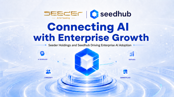
Seeder Holdings Evolves from Marketing and Business Growth Services into an AI Technology Company
Combining years of branding and market experience with enterprise AI solutions and the Seedhub AI Marketplace
Malaysia, 30th Jul 2026 — Seeder Holdings Sdn. Bhd. has officially entered a new phase of corporate development, evolving from its earlier focus on digital marketing, brand communication, content production and business growth services into a Malaysia-based AI technology company focused on enterprise AI transformation and AI solutions.
Over the years, Seeder Holdings has supported businesses in brand building, market development, customer engagement and commercial growth. Through this experience, the company developed a practical understanding of market demand, consumer behaviour and business operations.
As generative AI, AI agents and automation technologies continue to advance, artificial intelligence is moving beyond content creation and becoming increasingly relevant to customer service, sales follow-up, internal knowledge management, workflow automation and day-to-day business operations.
In response to this shift, Seeder Holdings is combining its existing strengths in marketing, content and business growth with AI technology, enterprise systems, talent development and cloud infrastructure to help businesses move from understanding AI to applying it effectively.
Extending Marketing Experience into Enterprise AI Applications
Seeder Holdings’ transformation does not mean leaving behind its previous business foundation. Instead, the company is upgrading its existing capabilities into a more complete range of enterprise AI services.
In the past, Seeder Holdings primarily helped businesses improve brand visibility, customer reach and commercial growth. Today, the company applies AI agents, AI automation and customised enterprise systems to improve customer response efficiency, optimise sales follow-up, accelerate content and video production, strengthen internal knowledge management and reduce repetitive operational work.
The company also extends its marketing and branding experience into AI GEO and digital channel strategies, helping businesses improve visibility across AI-powered search platforms and online channels.
Seeder Holdings aims to make AI more than a standalone tool. Its goal is to turn AI into a practical business capability that organisations can use, manage and continuously develop to create long-term value.
From Planning to Implementation, Building Practical Enterprise AI Capabilities
Seeder Holdings currently focuses on enterprise AI transformation consulting, AI agents, workflow automation, customised enterprise AI systems, AI customer service, sales assistants, content and video production, AI GEO, CRM and API integration, cloud deployment, AI model integration and GPU computing support.
For each project, Seeder Holdings begins by understanding the organisation’s existing challenges, systems, workflows and business objectives. The company then recommends suitable AI products or develops customised solutions based on actual operational needs.
Seeder Holdings also supports technology integration, testing, deployment and team training to ensure that AI becomes part of daily business operations rather than remaining at the concept or trial stage.
Seedhub Connects AI Products, Users and Business Opportunities
As the flagship AI platform of Seeder Holdings, Seedhub is positioned as:
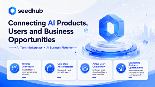
An AI Tools Marketplace and AI Business Platform
Seedhub is not a single AI product. It is a platform that connects AI tools, users, developers, enterprises, affiliates and business partners.
For users, Seedhub brings together different AI products, making it easier to discover and use suitable tools. For developers, the platform provides product listing and sales opportunities. For enterprises, Seedhub offers more advanced AI automation solutions. Affiliates can promote products and earn commissions, while brand and resource partners can pursue deeper platform collaboration.
The platform is designed to address three common market challenges: users may not know which AI tools to choose, developers may have products but lack customers and sales channels, and AI products and market demand remain fragmented.
Seedhub connects the people who build AI, use AI, promote AI and bring market resources together.
Making AI Products Easier to Discover, Purchase and Promote
Seedhub focuses on five core functions.
First, it brings together different AI tools so users can discover and compare suitable products more easily. Second, it provides developers with a platform to list and sell AI products. Third, it allows affiliates to promote products and earn commissions from successful transactions. Fourth, it helps enterprises adopt AI automation and enterprise-level solutions. Fifth, it connects brands, customer resources and business partners for deeper collaboration.
The platform connects products, traffic, transactions and services so that AI products are not only developed, but also seen, purchased, promoted and used.
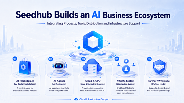
Building a Complete AI Product and Business Ecosystem
Seedhub is more than an AI marketplace. It also brings together AI agents, cloud and GPU infrastructure, affiliate systems, and partner or white-label collaboration models.
AI agents can help users complete tasks rather than simply respond in conversation. Cloud and GPU resources provide the computing foundation needed for AI products to operate. The affiliate system enables partners to promote products and earn commissions, while partner and white-label models support deeper brand and platform collaboration.
Seedhub will continue to onboard more AI products, developers and partners, expanding the range of solutions and commercial connections available through the platform.
Building a Long-Term Platform Connecting AI and Business
Seedhub’s value goes beyond selling individual AI tools.
The platform serves users, developers, affiliates, enterprise customers and business partners, while creating multiple commercial pathways through products, platform services, enterprise solutions, computing resources and partnership models.
In the long term, Seedhub aims to become an entry point for AI products and AI business opportunities, enabling more participants to take part in the AI economy and supporting stronger collaboration between technology, markets and commercial resources.
About Seeder Holdings
Seeder Holdings is a Malaysia-based AI technology company specialising in enterprise AI transformation, AI agents, AI automation, AI education and cloud AI solutions.
Building on its experience in digital marketing, brand communication, content production and business growth, the company provides end-to-end support across AI consulting, product matching, technology integration and corporate training.
Seeder Holdings helps businesses improve efficiency, strengthen customer experience and build long-term AI capabilities.
Official Website:
https://seederholdings.com/
LinkedIn:
https://www.linkedin.com/company/seeder-holdings
Office Address:
A26-1, A26-2 & A26-3, The Vertical Business Suites, Bangsar South, 59200 Kuala Lumpur, Malaysia.
Media Contact
Organization: Seeder Holdings Sdn Bhd
Contact Person: Mr.Loke
Website: http://www.seederholdings.com/
Email: Send Email
Country:Malaysia
Release id:47723
The post Seeder Holdings Evolves from Marketing and Business Growth Services into an AI Technology Company appeared first on King Newswire. This content is provided by a third-party source.. King Newswire makes no warranties or representations in connection with it. King Newswire is a press release distribution agency and does not endorse or verify the claims made in this release. If you have any complaints or copyright concerns related to this article, please contact the company listed in the ‘Media Contact’ section
About Author
Disclaimer: The views, suggestions, and opinions expressed here are the sole responsibility of the experts. No Digi Observer journalist was involved in the writing and production of this article.
Press Release
Prospexia Outsourcing Launches 50 Percent Off for U.S. Businesses Hiring On Site Filipino Virtual Assistants and Call Center Teams in Sorsogon City
Philippines BPO Pioneer with 10M Plus Calls and 210 Plus Global Partners Opens New Client Slots from Its Managed Sorsogon City Facility as U.S. Demand for Accountable Offshore Talent Surges in 2026
Philippines, 30th Jul 2026 — Prospexia Outsourcing, a premier Philippines based business process outsourcing company, has launched a limited time initiative offering 50 percent off standard hourly rates for the first 12 months. U.S. businesses can book a discovery call to access fully managed Filipino virtual assistants, customer service representatives, sales development representatives, and appointment setters who work on site at the company’s professional facility in Sorsogon City, Philippines. Unlike virtual assistant agencies that dispatch freelancers working from home with no oversight, Prospexia recruits, trains, and deploys elite Filipino talent inside a managed, supervised, on site environment where quality assurance, real time coaching, and direct management happen daily.
The promotion arrives as the Philippine business process outsourcing industry reaches a projected 42 billion dollars in revenue and nearly 2 million professionals in 2026. While many VA agencies have rushed to cut costs by sending home based freelancers to clients with minimal oversight, Prospexia Outsourcing has doubled down on its physical operations in Sorsogon City. The company operates a fully staffed facility where agents report to work, use enterprise grade internet and phone systems, and are managed by on site team leads and QA coaches.
“The work from home VA model is a disaster for American business owners,” said Chris Diaz, CEO and Founder of Prospexia Outsourcing.
“These agencies sell you a dedicated virtual assistant, then farm your work out to some freelancer sitting in a noisy living room with spotty internet, zero supervision, and no accountability. When that freelancer disappears, the agency swaps in another random person and bills you for the downtime. At Prospexia, our agents work on site in our Sorsogon City facility. They clock in. They have managers walking the floor. They have IT support three feet away. They have QA coaches listening to calls in real time. That is why our client satisfaction rate is 94.5 percent and why we have handled 10 million calls without a single contract dispute.”
Diaz continued, “American business owners think they are getting a professional team when they hire a remote Filipino virtual assistant through some marketplace. What they are actually getting is an unsupervised freelancer juggling three clients at once, dropping calls because the neighbor is renovating, and vanishing for days with no explanation. That is not outsourcing. That is gambling. We do the opposite. Our agents work in a controlled, professional environment with redundant internet, noise canceling headsets, backup power, and direct supervision. They stay with our clients for years because we treat them like professionals, pay them above market rates, and give them a real career path inside a real facility.”
What U.S. Businesses Get with Prospexia Outsourcing
Founded in 2012, Prospexia Outsourcing has supported 210 partnered companies and handled 10 million calls, maintaining a 94.5 percent customer satisfaction rate. The company provides fully managed on site teams from its Sorsogon City facility across the following categories:
Customer Service Outsourcing. Inbound and outbound call center support, omnichannel customer care, live chat, email management, and help desk operations delivered by on site Filipino customer service representatives under direct floor management.
Sales Development and Cold Calling. Trained Filipino SDRs and cold callers for insurance agencies, real estate, merchant cash advance, SaaS, and home service businesses operating on site with professional headsets, redundant internet, and quiet workstations.
Appointment Setting and Calendar Management. Dedicated on site Filipino appointment setters who qualify leads, book discovery calls, and manage executive calendars using the client’s preferred CRM and scheduling tools.
Virtual Assistant Services. Administrative support, data entry, CRM management, billing, document processing, and back office operations delivered by skilled Filipino virtual assistants working on site inside a managed facility, not from home.
Healthcare and Insurance Support. Insurance verification, patient surveys, medical billing, and healthcare administrative services handled by trained on site Filipino agents compliant with U.S. standards.
ESL and Accent Training. All on site agents complete Prospexia Academy training in U.S. neutral accent English, American business culture, and industry specific terminology before deployment. Quality assurance monitoring and daily reporting are conducted on site with the same rigor as any premium call center.
Unlike virtual assistant agencies that bill you for invisible home based workers with no oversight, Prospexia Outsourcing operates on a flexible month to month model with full transparency. New clients who book a discovery call at https://calendly.com/connect-prospexiaoutsourcing/discovery-call lock in 50 percent off standard rates for 12 months, with full on site management, quality assurance monitoring, daily reporting, and free agent replacement included.
Why U.S. Companies Choose On Site Filipino Virtual Assistants in Sorsogon City in 2026
Managed Facility with Direct Oversight. Prospexia agents work inside a professional Sorsogon City facility with on site team leads, QA coaches, and IT support. Every agent is visible, accountable, and managed in real time. There are no mystery freelancers hiding behind a screen.
English Proficiency and Cultural Alignment. The Philippines ranks second in Asia for English proficiency. Filipino virtual assistants share deep cultural familiarity with U.S. business norms, consumer behavior, and communication styles, resulting in smoother customer interactions and higher conversion rates.
Major Cost Savings Without the Home Based Risk. U.S. businesses save 50 to 75 percent on labor costs by outsourcing to on site Filipino virtual assistants. Because Prospexia operates from Sorsogon City rather than expensive Metro Manila, those savings pass directly to clients while agents earn competitive salaries in a professional environment.
24/7 Coverage and Lower Turnover. On site Filipino teams provide seamless coverage across all U.S. time zones from the Sorsogon City facility. The professional environment provides structure, career development, and community that home based freelancers rarely get. Prospexia clients benefit from longer tenured agents who know their products, systems, and customers intimately.
Specialized Industry Expertise. Prospexia serves verticals including insurance, real estate, healthcare, merchant cash advance, SaaS, legal services, marketing agencies, e commerce, and home services. Each on site agent receives customized training tailored to the client’s industry, product, and sales process.
“Most virtual assistant agencies want you to believe that home based freelancers are the future,” Diaz stated. “That is a lie told by companies too cheap to run a real facility. Our on site Filipino virtual assistants and sales agents deliver superior professionalism, accent quality, and CRM skills because they work in a real office with real managers, real training, and real accountability. In every case, they outperform home based freelancers because they are more focused, more supported, and more committed. Outsourcing to the Philippines in 2026 is not about finding the cheapest freelancer on the internet. It is about building a scalable, accountable revenue engine. Our agents do not just answer phones. They become a true extension of your brand, working on site in Sorsogon City but fully embedded in your business.”
How to Book Your Discovery Call and Claim 50 Percent Off
U.S. businesses ready to hire on site Filipino virtual assistants, managed call center agents, or professional sales teams can book a no obligation discovery call directly with the Prospexia leadership team. Prospexia evaluates the client’s workflow, identifies the ideal on site talent match, and can deploy trained agents from its Sorsogon City facility within 48 hours of approval.
Book your discovery call now: https://calendly.com/connect-prospexiaoutsourcing/discovery-call
Email: connect@prospexiaoutsourcing.com
Website: https://prospexiaoutsourcing.com/
Phone: (888) 682-4703
About Prospexia Outsourcing
Prospexia Outsourcing is a Philippines based business process outsourcing company specializing in on site customer service, sales development, appointment setting, virtual assistance, and healthcare support for U.S. and international clients. Established in 2012 and led by CEO Chris Diaz, the company combines over a decade of operational excellence with a proprietary training academy that prepares on site Filipino talent for U.S. neutral accent communication, CRM proficiency, and industry specific workflows. Unlike virtual assistant agencies that rely on unsupervised home based freelancers, Prospexia operates a fully managed facility in Sorsogon City where agents work under direct supervision with enterprise grade infrastructure. With 210 partnered companies, 10 million calls managed, and a 94.5 percent client satisfaction rate, Prospexia Outsourcing delivers enterprise quality results at smarter costs with no long term contracts, no setup fees, and 24/7 availability.
Media Contact
Organization: Prospexia Outsourcing
Contact Person: Chris Diaz
Website: https://prospexiaoutsourcing.com/
Email: Send Email
Country:Philippines
Release id:47717
The post Prospexia Outsourcing Launches 50 Percent Off for U.S. Businesses Hiring On Site Filipino Virtual Assistants and Call Center Teams in Sorsogon City appeared first on King Newswire. This content is provided by a third-party source.. King Newswire makes no warranties or representations in connection with it. King Newswire is a press release distribution agency and does not endorse or verify the claims made in this release. If you have any complaints or copyright concerns related to this article, please contact the company listed in the ‘Media Contact’ section
About Author
Disclaimer: The views, suggestions, and opinions expressed here are the sole responsibility of the experts. No Digi Observer journalist was involved in the writing and production of this article.
HandwritingToExcel.com Launches AI Tool to Automate Handwriting to Excel Conversion
Seeder Holdings Evolves from Marketing and Business Growth Services into an AI Technology Company
Prospexia Outsourcing Launches 50 Percent Off for U.S. Businesses Hiring On Site Filipino Virtual Assistants and Call Center Teams in Sorsogon City
Benzinga Money Article Discusses How to Become Part of the 12% of Retirees Who Have Achieved the Recommended $550,000 Minimum Retirement Savings Threshold
Apu Apustaja Conquers New York with Lively Street Ads, Including Times Square Billboard
Bay Smokes Maintains Quality Amid Legislative Changes in the Hemp Industry


-
Press Release6 days ago
Post Oak Group Advises on Successful Sale of Philadelphia-Based Computer Solutions Business to Search Fund-Backed Acquirer
-
Press Release6 days ago
Harborstone Point Advisors Expands Revenue Cycle Management and Financial Advisory Services for Behavioral Health Organizations
-
Press Release6 days ago
Anime Expo 2026 Jaadugar A Witch in Mongolia Reveal Behind-the-Scenes Insights and Anime Secrets
-
Press Release5 days ago
All Thingz Electric Expands EV Charger Installation Services Across South Orange County to Meet Growing Demand
-
Press Release5 days ago
23 Years, One Question: “Diaoyu Dao: Small Islands, Big Stakes” — A CGTN Documentary
-
Press Release5 days ago
RELVE Q2 Report Reveals AI Hype Gap After Analyzing 1.59M Data Points and 23,000 Tools
-
Press Release4 days ago
Biomaser and LatinLook Strengthen PMU Partnership in Argentina
-
Press Release5 days ago
Ken Behr Turns Years as a DEA Cooperating Source Into True Crime Podcast Crime Nightly